Intel Proposes 80 Core… For Your Laptop

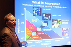
Intel says it has developed an 80-core microprocessor chip that could enable PCs and chip-enabled devices to perform Teraflop level computing. The company will offer more details of its research in a series of scientific papers at the annual Integrated Solid State Circuits Conference this week in San Francisco. The chip maker says the result of providing such chips to the market could help usher in artificial intelligence, instant video communications, photo-realistic games, multimedia data mining and real-time speech recognition. The demonstration model unveiled last week in San Francisco, however, is not a prototype for a product. Still, the company says the technology would be built into future chips designs. Jason Lopez of PodTech spoke with Intel CTO Justin Rattner.
Here’s an interesting video produced by Intel at their research facility in Hillsboro, Oregon featuring engineers who are working on 80-core technology.
Related Stories: IntelMooresLaw
More Information:
Intel Tera-Scale Research (80-Core animation
available on this site)
Transcript:
Host: Jason Lopez – PodTech
Jason Lopez – PodTech
What’s better than a teraflop computer in a room? Obviously, a teraflop computer on a chip. What this is a production prototype of the world’s first teraflop on a chip die. Each of these dies has 80 simple floating-point cores on them with stacked SRAM. There are over 80 die on this wafer. Each 80-core die is capable of a teraflop performance with the ability to transfer terabytes -per-second of data between the cores and the stacked SRAM. Now it’s a prototype, but we think that the capability embodied by this prototype chip is going to be commercially available in a five-year window and that allows us to do some very amazing things.
This kind of performance gives us, the first time capability to imaging things like real-time video search or real-time speech translation from one language to another. Now, at the most fundamental level, the thing that makes all this work, the thing that makes this come alive is the transistor. And a lot has changed in the world of computing, but there’s been one constant, and that’s Moore’s Law.
Video plays — We hear a lot about Moore’s Law, but I don’t think that most people are aware of what doubling every two years really means.
(Music)
Mark Bohr – Intel
When I first joined Intel, the smallest transistor dimensions were about 3 microns. Today the smallest dimensions are around 30 nanometers, a 100 times smaller. Over the years, our process technology has changed dramatically. Our wafer sizes have grown from a 3-inch diameter in 1978 to today’s 12-inch diameter, and we have switched from bipolar to NMOS to CMOS technology, and more recent innovations have been “locate dielectrics”, copper interconnects, and strained silicon transistors.
In each case, the goal was to improve performance and to reduce power. So, while the concept of Performance-per-watt is somewhat new to the industry, power considerations have been a focus for Intel all along.
Yan Borodovsky – Intel
Lithography is how we reproduce, the design patterns on the chip. Of all the manufacturing steps, it is the most complex and most expensive. Patterns created by a chip designer are first etched into the mask then transferred by shining light through the mask onto the wafer. The process requires the most advanced lenses known to mankind. At the Intel we have a huge advantage over our competitors because we design and make our masks in-house. Our mask teams collaborate closely with our patterning teams to develop resolution, enhanced capability, to deliver higher-density patterning, earlier and with lower cost.
Mark Bohr – Intel
Moore’s Law isn’t like a natural law. It doesn’t just happen. We began working on 65-nanometer over five years ago. And are now working on processes for use five years or more from now. Gordon Moore formulated a law. Now it’s up to us to keep him honest.
Copyright ©2006 PodTech.net. All rights reserved. Privacy policy
Posted in:
Artificial Intelligence, Connected Social Media, Corporate, Intel, Intel Moore's Law, Intel PCA Past and Future, Technology


