Testing out Intel’s new 45 nanometer processors
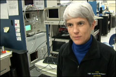
Kelin Kuhn is the 45 nanometer device group manager. She runs one of Intel‘s most important test labs where Intel figures out what needs improvement. Intel’s profitability rests on her shoulders because if a fab isn’t yielding enough good chips per wafer, Intel will make a lot less money. Get a look inside the lab and how Intel tests out its 45 nanometer chips and understand why these new chips will use less power than older designs.
Related Stories: IntelMooresLaw
Transcript:
Host: Robert Scoble – ScobleShow
Guest: Kelin Kuhn – Intel
Robert Scoble – ScobleShow
Yeah, so who are you. Who are you just talk to me.
Kelin Kuhn – Intel
Okay.
Robert Scoble – ScobleShow
Forget the cameras here.
Kelin Kuhn – Intel
Okay. I am Kelin Kuhn, I am the 45 nanometer Device Group Leader for Intel.
Robert Scoble – ScobleShow
Wow!
Kelin Kuhn – Intel
I am in-charge of the transistor architecture for 45 nanometer.
Robert Scoble – ScobleShow
Wow! And where are we?
Kelin Kuhn – Intel
We’re in the device lab which is…
Robert Scoble- ScobleShow
Come over here, so I can get a little look at what we’re looking out here.
Kelin Kuhn – Intel
So, this is where we test transistor devices for the technology, and here in the background we just — let me start over – I lost it. Here in the background we have a test station with (Inaudible) wafer on it. In fact, we just I’ll ask one of my technicians to move off for a second so we can show you the station.
Robert Scoble- ScobleShow
Okay.
Kelin Kuhn – Intel
You can basically see the wafer probes, the wafer so here, we’ve got the split charts setup and we’re beginning to do actual measurements on the wafer.
Robert Scoble – ScobleShow
Okay.
Kelin Kuhn – Intel
This kind of technology with a very advanced architecture we use, requires very careful measurements and so we supported a lot of hardware in order to make the types and accuracy of measurements we need.
Robert Scoble – ScobleShow
Right and what are the people doing in this lab specifically, what are they trying to look for or what are they doing — what are they tagged with?
Kelin Kuhn – Intel
Well, if you think about what we’ve done in the technology and 45 nanometers what we’ve introduced is basically the world’s first High-K/Metal gate transistor.
Robert Scoble – ScobleShow
Yeah.
Kelin Kuhn – Intel
If you think about High-K/Metal gate, what that does is that buys you some advantages in performance and in leakage over the conventional technology.
Now, High-K/Metal gate is a very unusual gate architecture. What we’ve done here is we’ve introduced a hafnium dielectric instead of the silicone dioxide dielectric and we’ve gotten some significant advantages particularly in leakage. Now, if you think about it, if you’ve spent many years measuring silicone dioxide devices with one kind of leakage and one kind of capacity performance and you start measuring these new devices, it requires some change in how we do business.
Robert Scoble – ScobleShow
Yeah. What is the leakage percentage of different…?
Kelin Kuhn – Intel
Well, it’s a good question. The kinds of number were seen is we’re seeing about a 10X reduction in gate leakage for this technology.
Robert Scoble- ScobleShow
Which means to the person at home lets heat coming off the chip and no power?
Kelin Kuhn – Intel
Well, if you think about it, think about the last time you bought a laptop, right?
Robert Scoble- ScobleShow
Yeah.
Kelin Kuhn – Intel
You probably bought it for some combination of, it will run my favorite software which is performance and our transistors will deliver 20% more performance than the previous technology and you also probably bought it for something like I can fly across United States on a battery. Well, gate leakage is one of the main components of transistor leakage and that means power and that means you’re not sucking your battery and so a 10X reduction in gate leakage has a lot of impact. It might make the difference is to whether you could fly from here to Atlanta or from here to New York.
Robert Scoble – ScobleShow
And it make the huge difference to somebody like Google or Yahoo! or Microsoft who has a hundreds of thousands of machine with your processor.
Kelin Kuhn – Intel
That’s exactly right and the High-K/Metal gate technology with the significant reduction in gate leakage is especially valuable when the transistors are idle because if you think about gate leakage in a transistor architecture, if the transistor isn’t doing a whole heck of a lot it’s still leaking through the gate, well if you can reduce the gate leakage, you’re that much better off.
Robert Scoble – ScobleShow
Interesting! And so what is this machine behind in here?
Kelin Kuhn – Intel
Well, this is just the Probe Station and what we do and you can actually see it here is we have this very fine needle like probes that go over it and…
Robert Scoble – ScobleShow
You just jump over here so I have to say in microphone and audio.
Kelin Kuhn – Intel
So, we have these very fine needle like probes that go over and drop on the wafer. Now, the picture isn’t very exciting because these are just the probe heads when they drop and you can see the little place where the probes have been. But then what we do is then the electrical signals come through these probes and we can setup with the various hardware we have exactly the signal that we want to go in there in order to do voltage or current or capacitance or leakage or whatever we want to do.
This type of station here is typically used for measurements when we want to do something it’s a little non-standard because you can see the folks can sit here and type in on the computer specialized types of measurements to do non-routine things. Some of the other hardware here is more automated. But, this area is the area that we use for the developmental activities.
Robert Scoble – ScobleShow
Right. What is the rest of this lab for? What kinds of things that you’re doing in the rest of the lab that you can tell me about? I am not sure everything is top secret at Intel.
Kelin Kuhn – Intel
Everything is top secret. What we can do on the rest of the lab is, there are several technologies supported here at the same time. This technology 45 nanometers is just entering the phase where we begin to transition the technology off to the high volume manufacturing room. Over one corner of the lab we have the next generation 32 nanometers where people are trying to figure out what the transistor architecture is, and in another corner of the lab we have the last technology which is 65 nanometers where they are doing some high volume work and trying to figure out things like, how many time the probes can sit on the wafer before the probe get damaged and that sort of stuff.
Robert Scoble – ScobleShow
Interesting!
Kelin Kuhn – Intel
So, in this kind of environment typically we have three simultaneous technologies running, the one we’re doing, the one we just did that’s usually making us money and the one we’re about to do that’s in some sort of a research/(Inaudible) probe.
Robert Scoble – ScobleShow
Yeah. Well, thanks for spending a little bit of time. Is there anything else that I should know or viewers at home should know about the lab and the work you and your team does?
Kelin Kuhn – Intel
Well, I think one of the most important messages that I could send is that High-K/Metal gate is probably the most significant transistor architecture change probably in the last 30 years, certainly in my adult life. I can also say that I think Intel is probably the only company that could have done it because many things in this technology have been challenging, trying to make the leakage requirement, the performance requirements, or the role requirements in such a novel system because this is basically a hafnium-based dielectric, has really been something that has been out of the normal for a transistor development side.
Robert Scoble – ScobleShow
How long have you been here in Intel?
Kelin Kuhn – Intel
I have been here a decade.
Robert Scoble – ScobleShow
A decade?
Kelin Kuhn – Intel
Yeah.
Robert Scoble – ScobleShow
Is that the craziest thing you’ve seen Intel try to do in a decade or how does this match up to other challenges that Intel has met?
Kelin Kuhn – Intel
Well, we have done some pretty surprising things and each generation at the beginning of the technology cycle I look at the design roles, which is the basic architecture and I go — Uh… we couldn’t possibly do this and then as the technology develops all of a sudden there is one day when all looks pretty easy and then you go to the next one, but I will confess all the High-K/Metal gate technology has been the most challenging technology I have experienced at Intel and there were many days in the developmental cycle when I said, “Oh no, this couldn’t be done” and it’s been really a spectacular experience to be able to do this.
Robert Scoble – ScobleShow
Who on your team would you like to give credit to for helping you out?
Kelin Kuhn – Intel
Oh! I think the credit definitely should go to my two mentors at Intel Mark Bohr who is the senior fellow who is actually introducing this session and then my immediate supervisor who is Carl’s (ph) administrator who is the 1266 program manager and I owe both gentlemen a significant amount of thanks for their help to me during this technology cycle.
Robert Scoble- ScobleShow
Well, thanks for spending a few minutes with me explaining what you do.
Kelin Kuhn – Intel
All right.
Copyright ©2006 PodTech.net. All rights reserved. Privacy policy
Posted in:
Connected Social Media, Corporate, Enterprise 2.0, Intel, Intel Moore's Law, ScobleShow, Technology